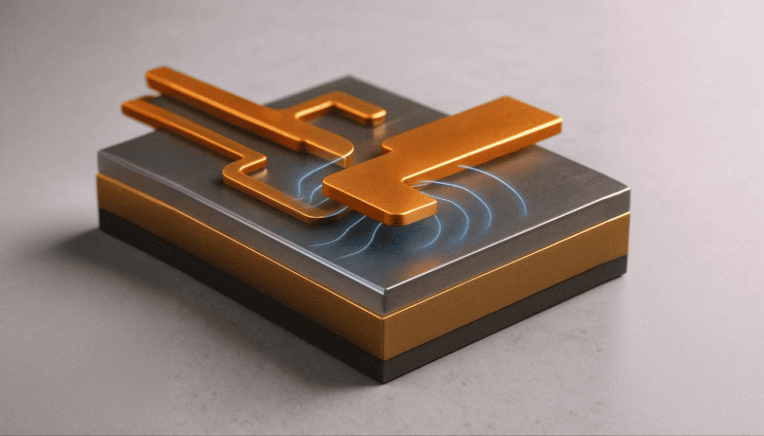
A large and continuous ground plane is a crucial practice to minimize impedance, reduce EMI, and mitigate signal coupling issues in thin film devices. A ground plane provides a low impedance path for the return currents of the signals, which helps to minimize the loop area, reduce ground noise, and enhance signal integrity by maintaining a stable reference potential. It also acts as a shield, reducing electromagnetic interference (EMI) by providing an effective ground return path and preventing the propagation of unwanted electromagnetic fields. Additionally, a well-designed ground plane helps to isolate and minimize crosstalk between adjacent signal traces by providing a solid reference plane that reduces the electromagnetic coupling between traces.
A large and continuous ground plane is a crucial practice to minimize impedance, reduce EMI, and mitigate signal coupling issues in thin film devices.
- Low Impedance Path: A large ground plane provides a low impedance path for the return currents of the signals. This helps to minimize the loop area, reduce ground noise, and enhance signal integrity by maintaining a stable reference potential.
- EMI Mitigation: A continuous ground plane acts as a shield, reducing electromagnetic interference (EMI) by providing an effective ground return path and preventing the propagation of unwanted electromagnetic fields.
- Crosstalk Reduction: A well-designed ground plane helps to isolate and minimize crosstalk between adjacent signal traces by providing a solid reference plane that reduces the electromagnetic coupling between traces.
- Thermal Management: The large metal area of the ground plane helps to dissipate heat from the components, which is especially important for high-power devices.
- Reliability: By providing a low impedance path for the return currents, the ground plane helps to reduce the risk of ground bounce and other signal integrity problems.
Achieving a Large and Continuous Ground Plane
Single Solid Plane
- Design the substrate with a single, continuous ground plane that covers the majority of the substrate area.
- Avoid splitting or discontinuities in the ground plane unless necessary for specific circuitry requirements.
Minimize Ground Plane Splitting
- If splitting the ground plane is unavoidable, ensure proper routing and return paths between the split sections.
- Implement stitching vias or bridges to maintain connectivity and reduce impedance between the split ground planes.
Avoid Signal Traces in the Ground Plane
- Keep signal traces away from the ground plane to minimize coupling and interference.
- If traces must cross the ground plane, use a bridge or clearance in the ground plane to maintain isolation and prevent coupling.
Component Placement
- Plan the placement of components on the substrate to maximize the coverage of the ground plane.
- Avoid blocking the ground plane with components or routing traces that would limit its continuous nature.
Via Placement
- Strategically place vias to connect the top and bottom ground layers, ensuring a low impedance return path and maintaining a continuous ground plane throughout the substrate.
- Use an adequate number of vias to minimize ground impedance and optimize the return paths.
Signal Layer Arrangement
- Consider the arrangement of signal and ground layers in a multilayer substrate design.
- Place the ground layers adjacent to signal layers to provide efficient return paths for signals and reduce crosstalk.
High-Quality Connections
- Ensure proper grounding connections between the ground plane and the components, such as using vias with sufficient diameter, low impedance paths, and good solder joints.
Use a Low-Loss Substrate
- The substrate material can have a significant impact on the impedance of the ground plane.
- Choose a substrate material with a low dielectric constant (Dk) and low loss tangent to minimize the impedance of the ground plane.
Optimize the Ground Plane Thickness
- The thickness of the ground plane can also affect the impedance.
- A thicker ground plane will have lower impedance, but it will also be heavier and more expensive.
- The optimal thickness will depend on the specific application.
Use Stitching Vias
- Stitching vias can be used to connect the top and bottom ground layers, which helps to improve the continuity of the ground plane and reduce impedance.
Apply a Solder Mask
- A solder mask can help to protect the ground plane from corrosion and improve the electrical conductivity of the ground plane.
In conclusion, a large and continuous ground plane is a crucial practice to minimize impedance, reduce EMI, and mitigate signal coupling issues in thin film devices. By following the tips outlined in this article, you can design a large and continuous ground plane that will help to improve the performance, reliability, and EMI immunity of your thin film device.
Here are some of the key points to remember:
- A large ground plane provides a low impedance path for the return currents of the signals, which helps to minimize the loop area, reduce ground noise, and enhance signal integrity by maintaining a stable reference potential.
- A continuous ground plane acts as a shield, reducing electromagnetic interference (EMI) by providing an effective ground return path and preventing the propagation of unwanted electromagnetic fields.
- A well-designed ground plane helps to isolate and minimize crosstalk between adjacent signal traces by providing a solid reference plane that reduces the electromagnetic coupling between traces.
- The thickness of the ground plane can also affect the impedance. A thicker ground plane will have lower impedance, but it will also be heavier and more expensive. The optimal thickness will depend on the specific application.


Leave a Reply