There’s a quiet revolution happening beneath the chips we obsess over.
Not in the silicon itself — but underneath it.
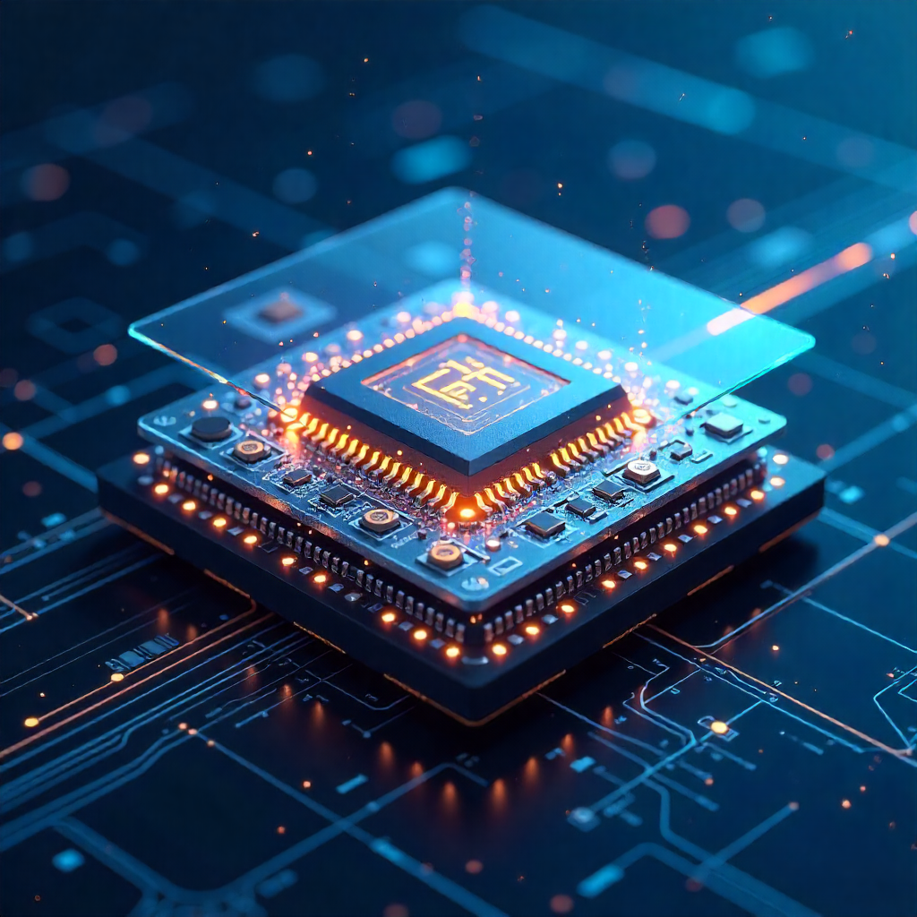
For decades, the substrate was the unsung hero of electronics — a silent base holding everything together. But as AI and high-performance computing stretch every physical limit, that humble layer has become the next battleground.
And glass — once dismissed as too fragile or too costly — is back in the spotlight.
Fundamentals Don’t Change — Only Attention Does
Glass substrates have always had exceptional fundamentals: flatness, dimensional stability, low dielectric loss, and high resistivity.
Those properties are tailor-made for high-speed signaling.
The reason glass faded from view wasn’t performance — it was timing and economics. In the 1990s, when interconnect density was modest and cost ruled, organic laminates won by being cheap and “good enough.” Glass simply couldn’t justify its price.
But AI workloads have changed the math.
Today’s accelerators move terabytes per second. A few microns of warpage or a tiny mismatch in thermal expansion can destroy alignment, yield, and reliability. Suddenly, the old fundamentals look like the future.
And as yields improve and equipment amortizes, glass doesn’t just perform better — it begins to make economic sense.
Invert the Problem
So, what’s breaking today’s packages?
Invert that question, and the answer appears.
Organic substrates warp under thermal cycling.
Silicon interposers are precise but costly and limited in size.
Ceramics are reliable but can’t scale to large panels.
What’s dimensionally stable like silicon, scalable like organic, and low-loss like ceramic?
Glass.
In the age of chiplets and co-packaged optics, glass isn’t an experiment anymore — it’s a logical evolution.
The Platform Beneath the Platform
Performance isn’t just about the chip — it’s about the entire stack.
Glass is the quiet foundation that lets that stack scale.
It enables tighter interconnect density, lower power per bit, and cleaner signal paths.
Demonstrations already show glass cores supporting sub-2-micron line-and-space features and finely drilled through-glass vias — precision that matters when thousands of signals move simultaneously at multi-gigahertz speeds.
The next wave of compute power won’t come only from faster chips.
It will come from shorter distances, cleaner interconnects, and lower parasitics.
Glass helps make that possible.
And no company will industrialize glass alone. Progress will come from co-development — materials innovators, design houses, and packaging fabs working together toward manufacturable precision.
Discipline Over Hype
Innovation without yield is just art.
Glass still faces its trials — reliable via formation, uniform metallization, adhesion control, and integration with bumping and inspection tools.
The winners will be the ones quietly grinding through yield curves, turning a fragile process into a repeatable one.
Manufacturing discipline, not marketing, is the true moat.
Context Creates Meaning
Glass substrates should be seen as the enabler of reliable performance scaling in AI and HPC systems.
That clarity — not novelty — is what turns a technology into a movement.
Glass isn’t an exotic science project. It’s what allows compute systems to grow without breaking their physical limits.
Antifragility in Engineering
Fragility depends on context.
Yes, glass can shatter if mishandled — but inside a well-designed package, it’s remarkably predictable. It doesn’t warp, creep, or fatigue. Under heat and vibration, that stability becomes an advantage.
In high-stress environments — from data centers to satellites to medical implants — consistency is often more valuable than brute strength.
Glass doesn’t resist chaos; it disciplines it.
When engineered properly, it stays true under extremes.
The Compounding Edge
Consistency compounds faster than intensity.
Glass won’t replace silicon or organics overnight.
But every yield improvement, cleaner via, and smoother surface compounds over time.
Once those incremental gains stack, cost curves bend — and what was niche becomes inevitable.
At Vajra Microsystems, we see glass not as a one-off breakthrough but as a compounding process curve — where patience and process mastery quietly build dominance.
The compounding curve rewards those who stay through the quiet years.
Why It Matters Across Industries
The beauty of glass is that its advantages echo across many domains.
In semiconductors, it provides a stable base for high-density chiplet architectures.
In photonics, its transparency enables optical interconnects and co-packaged optics.
In RF and millimeter-wave systems, its low dielectric loss keeps signals clean and phase-stable.
In medical implants, specific glass types offer hermeticity and biocompatibility.
And in space hardware, its dimensional stability under radiation and temperature extremes enhances reliability.
Different industries, one common theme: precision, stability, and calm under stress.
The Road Ahead
Yields must rise. Handling must improve. Inspection must mature.
But the direction is unmistakable.
As systems chase higher precision per watt, glass is no longer chasing relevance — it’s catching up to necessity.


Leave a Reply