Glass interposers are gaining traction in AI, RF, and chiplet packaging. Whether they perform depends almost entirely on one fabrication decision: how the vias are filled.
Interest in glass interposers has accelerated as AI infrastructure, advanced packaging, and heterogeneous integration place increasing demands on interconnect density, power delivery, and signal integrity. Glass interposers are one credible answer — but the performance gap between a good glass interposer and a poor one comes down to a decision made before a single redistribution layer is deposited: how are the vias filled?
Why glass in the first place
Glass brings a combination of properties that are genuinely hard to replicate in organic or silicon substrates. Low dielectric loss at high frequencies makes it attractive for RF and millimeter-wave designs. Its CTE can be tuned closer to silicon than most organic alternatives, reducing interfacial stress at the die. Surface smoothness supports fine-pitch lithography. And large-panel compatibility opens a path to manufacturing economics that silicon interposers cannot easily match.
The argument for glass is not that it is better in every dimension. It is that for dense chiplet integration, high-frequency RF, and heterogeneous packages, it offers a combination of properties no other substrate material currently matches.
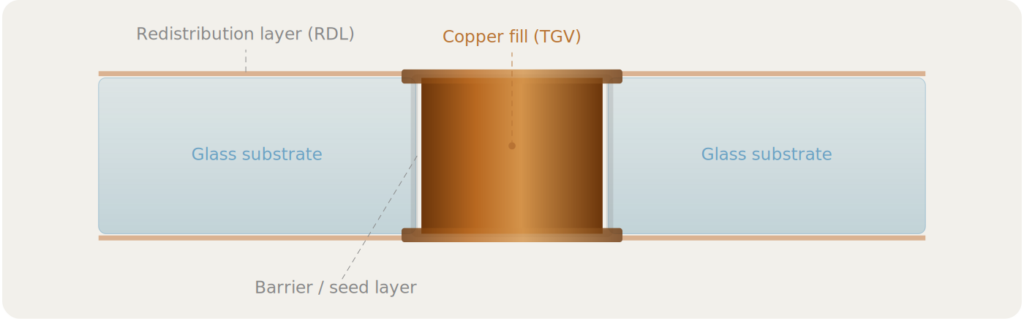
Lined vs. copper-filled: the core tradeoff
There are two standard approaches to making a via conductive. The difference between them propagates into every downstream performance metric.
Option A Lined via or Plated thru: Conductive material deposited via sidewalls only; center remains hollow. Lower process complexity. Adequate for some lower-density, lower-power applications. Leaves a non-planar surface that complicates fine-pitch RDL work.
Vajra approach Copper-filled via: Entire via volume electroplated with copper and planarized flush to the glass surface. Better resistance, better thermal conduction, better stress distribution, and a flat surface that makes downstream RDL processing cleaner and more reliable.
Common choice for demanding thermal and electrical requirements
Thermal: copper does the work glass cannot
Glass is a poor thermal conductor. In a passive routing interposer at low power, this is manageable. In an AI accelerator package or a high-power RF module, it is a real constraint.
Copper-filled vias partially offset this. Each completely filled via acts as a discrete thermal column through the glass, carrying heat away from the active device toward the package thermal interface. The effect scales with via count and placement density — which means thermal performance needs to be in the room when via layout decisions are made, not added as a review comment later.
Electrical: resistance and impedance control
For power delivery, filled vias provide lower resistance paths than hollow structures of the same diameter. In a dense via array carrying significant current, that difference accumulates across thousands of vias — separating a power delivery network that meets its budget from one that forces derating.
For signal vias, the absence of an air core reduces the impedance discontinuity at the via transition. As data rates push beyond 50 Gbps, via design is no longer a second-order concern. It is part of the signal integrity budget from the first schematic capture.
Mechanical: managing the glass-metal interface
Every temperature cycle loads the interface between glass and metal. CTE mismatch between copper and glass is real and must be managed by design. A lined via concentrates stress at the sidewall liner interface. A completely filled via distributes it through the copper column, which has better mechanical resilience under repeated cycling.
For applications with extended service life or significant thermal excursions — space, defense, medical implants — this is a reliability requirement, not a design detail.
Surface quality: what it enables downstream
Planarization after copper fill produces the surface that every subsequent process builds on: dielectric deposition, photolithography, RDL metallization. A non-planar starting surface — from a lined via or a poorly controlled fill process — introduces variation that compounds with each layer added above it. Fine-pitch RDL at 25 µm line and space or below requires a surface that is flat within tight tolerances before lithography begins.
Process discipline at the via level has an outsized impact on yield in the finished package. This is one of the areas where the choice of fabrication partner matters most.
The fabrication challenge: where it gets hard
Void-free copper fill in high-aspect-ratio vias requires careful control at every step. Getting it right consistently, across large panels, at tight dimensional tolerances, is a process engineering problem — not just an equipment selection.
1 Via formation — laser drilling, wet etching, or photosensitive glass processing. The choice affects sidewall quality, taper profile, and subsequent fill behavior.
2 Adhesion and barrier deposition — thin-film layers prevent copper diffusion into the glass matrix and anchor the metal stack to the sidewall.
3 Seed layer deposition — uniform coverage in high-aspect-ratio holes is non-trivial and directly determines plating uniformity.
4 Copper electroplating — bottom-up fill chemistry is critical. Void formation starts when plating closes off the via mouth before the bottom is fully filled. Chemistry, current density, and via geometry must all be matched.
5 Planarization (CMP) — removes overburden copper and produces the surface on which all downstream processing depends. Endpoint control is not optional.
The performance a glass interposer delivers in the field is largely determined during via fabrication. There is no downstream process that corrects a poorly filled via.
Beyond AI: where else are copper-filled TGVs used?
RF and microwave modules benefit from glass’s low dielectric loss and the predictable impedance of copper-filled vias — both matter when signal fidelity at millimeter-wave frequencies is the constraint. Photonic interposers require smooth sidewalls and precise vertical alignment; a filled-via architecture that planarizes cleanly makes both easier to achieve.
Medical devices, defense electronics, and sensor arrays share a common need: reliable vertical interconnect in a substrate that can survive thermal cycling and mechanical stress over a long service life. In all of these applications, the fabrication requirements are the same — void-free fill, clean planarization, and a process with enough discipline to repeat at yield. These are the types of manufacturing challenges that continue to drive development in advanced glass interposer technology.
What this means for your program
If you are evaluating glass interposers for an AI, RF, chiplet, or heterogeneous integration program, the via architecture is one of the first questions to resolve. The choice between lined and filled vias is not primarily a cost question — it is a performance question that touches thermal budget, power integrity, signal integrity, and long-term reliability simultaneously.
At Vajra, copper-filled TGV fabrication is part of our end-to-end glass process, running from design review through prototype, pilot, and early production. We share substrate runs where it makes sense to compress prototyping cost and timeline. If you are working through a glass interposer architecture and want to pressure-test the via strategy with someone who builds them, we are easy to reach.
Talk to our fabrication team
Describe what you are building. We will tell you quickly whether copper-filled TGVs are the right fit and what a prototyping engagement would look like.


Leave a Reply