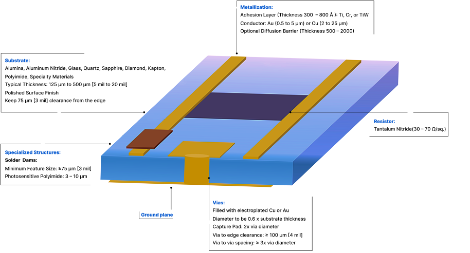
Vajra Microsystems | Precision Microfabrication for Advanced Technologies

Design. Fabricate.
Smarter.

Explore microfabrication solutions that grow with your innovation, from early-stage proof to production-ready.

Our Process

From concept to delivery, we ensure every step meets the
highest standards of precision and quality.

Design Review

Comprehensive analysis of
your specifications and
requirements

Prototype & Pilot Runs
Rapid prototyping and
small-scale production
validation
Production

Scalable manufacturing with consistent quality and
precision

Quality & Traceability

Rigorous testing and
complete documentation
throughout the process

Delivery & Support

Timely delivery with ongoing technical support and partnership

Advanced Materials We Work With

We enable innovation across microelectronics, RF, and medtech by offering next-gen materials with unmatched performance characteristics — designed to support early-stage prototyping through low-volume production.

Alumina
Al2O3
RF

Stable ceramic with excellent dielectric properties. Great for RF applications up to 30 GHz.

Aluminum Nitride
AlN
RFThermal

High thermal conductivity and RF compatibility — ideal for thermally intensive systems.

Glass
SiO2
Optical

Ultra-smooth, planar — perfect for interposers, 3D packaging, and microfluidics.

Sapphire
Al2O3
MedicalRFOptical

Chemically inert, optically transparent, biocompatible — used in medical + RF builds.

Quartz
SiO2
RF

Ultra-low dielectric loss and thermal expansion. Suitable for systems beyond 100 GHz.

Diamond
C
RFThermal

Top-tier thermal management and high-frequency performance. Ideal for power RF designs.

Kapton Film
PI
Medical

Ergonomic, flexible, and lightweight — used in medical imaging.

Silicon
Si
MEMS

A proven base for MEMS, sensor integration, and microfluidic platforms.

Polyimide
PI
Medical

For multilayer medical circuits supports lightweight, ergonomic builds with minimal assembly.

Advanced Materials We Work With

We enable innovation across microelectronics, RF, and medtech by offering next-gen materials with unmatched performance characteristics — designed to support early-stage prototyping through low-volume production.

Everything begins with context.

We listen closely to understand what you're building — and where it needs to perform. Every material, tolerance, and process we recommend is grounded in your real-world goals.

Why It Matters:
  • Matches process + material to end use
  • Avoids costly rework or delays
  • Sets you up for success in real conditions
Discovery Questions We Explore:
  • What’s the core function?
  • Signal, frequency, or noise sensitivities?
  • Power + thermal limits?
  • Rigid, flexible, or hybrid form factor?
  • Any reliability, safety, or regulatory needs?
Specifications Are Born Here

We don’t guess specs — we define them. From choosing AlN vs. sapphire to dialing in your metal stack, everything flows from clear constraints.

Key Takeaway

Good builds start with great questions.

Why Substrate Choice Matters

Substrates define electrical stability, thermal performance, and fabrication compatibility. A mismatch here compromises everything.

What We Ask
  • What frequency, loss, or impedance is needed?
  • Does the design require thermal management?
  • How important is planarity or surface polish?
  • Any cost, delivery, or supply constraints?
Specifications
  • Thickness: 125–500 µm
  • Edge Clearance: ≥ 75 µm
  • Surface: Low Ra for high-res patterning
Materials We Work With
  • Alumina: All-purpose ceramic
  • AlN: Great thermal conductivity
  • Quartz: For >100 GHz, ultra-low loss
  • Glass: Planar and scalable
  • Sapphire: Biocompatible and RF-capable
  • Diamond: Ultimate for thermal + RF performance
Key Takeaway

Treat substrates like performance enablers — not just structural platforms.

Why It Matters

Your metal stack isn’t just a technical detail — it’s a performance backbone. From conductivity to corrosion resistance, every layer has a job to do. We tailor each one to your application, not the other way around.

Let’s Think Together
  • Will you be wire bonding or soldering?
  • Are you pushing high current or packing tight lines?
  • Need it to survive harsh conditions or meet biocompatibility?

We’ll ask the right questions and guide material choices accordingly.

What We Often Use
Key Takeaway

There’s no one-stack-fits-all. We’ll build you one that’s just right — for your signals, your process, and your scale-up plan.

Why It Matters

The right vias improve thermal handling, enable 3D routing, and ensure stable RF and power delivery. Poor ones? They compromise everything from signal to yield.

What We'll Ask
  • Do you need thermal sinks, grounding, or vertical interconnects?
  • Should the vias be open or filled? With Cu or Au?
  • How close are features to the edge — and is CMP required?

These answers shape the machining and layout strategy.

Our Go-To Specs
  • Via Ø ≥ 60% of substrate thickness
  • Aspect Ratio < 0.6
  • Pad Ø ≥ 2× via Ø
  • Post-fill Planarity: ±7 µm
  • Edge Clearance: ≥100 µm
  • Include vent holes when filled.
Process Options
  • Fill: Copper (for thermal), Gold (for corrosion resistance)
  • Machining: Laser or mechanical — based on material
  • Polishing: CMP for alumina, soft polish for sapphire
Key Takeaway

Good vias make or break high-density layouts. We help you get them right — structurally, electrically, and thermally.

Why It Matters

Polyimides define how signals are routed, protected, and insulated. The right stack ensures your device handles heat, stress, and scale — especially in RF, medtech, or 3D builds.

What We’ll Explore Together
  • Are you building multilayer or flexible circuits?
  • Will the device face thermal or chemical stress?
  • Soldering, wirebonding — or both in the same stack?

We use these answers to guide your PI materials and thicknesses.

Design Guidelines We Follow
  • PI Thickness: 4–13 µm
  • Solder Dam: 3–7 µm tall
  • Edge Clearance: ≥ 75 µm
  • Alignment Tolerance: ± 3–5 µm
  • Thermal Limit: Up to 300 °C
Process Options We Offer
  • Photosensitive PI: Fast, patterned dielectric
  • Etchable PI: Plasma-routing flexibility
  • Kapton®: Biocompatible flex
  • Solder Dams: NiOx, TiW, or polyimide
Key Takeaway:

A smart polyimide stack gives you more functionality per square millimeter — without compromising reliability.

Why It Matters

Selective coatings prevent corrosion, reduce field failure, and add longevity — without interfering with connectors, probe points, or RF interfaces.

What We’ll Ask
  • Will the device face moisture, dust, or biocontamination?
  • Do any pads, test points, or RF ports need to stay exposed?
  • Will rework or probing be needed after coating?
Specifications:
  • Coating Thickness: 25–125 μm
  • No-Coat Clearance Zones: Must be defined
  • Application: Masked or selective-spray
Design Guidelines
  • Thickness: 25–125 µm
  • Define no-coat zones early in layout
  • Application: Masked or selective spray depending on geometry
Material Options
  • Acrylics: Fast and cost-effective
  • Parylene: Pin-hole free, excellent for medical
  • Epoxies: Rugged and chemical-resistant
Example Use Case

An RF module where the body is coated, but edge connectors are left open for post-fab tuning.

Key Takeaway

Coating isn’t all-or-nothing. We help you strike the right balance between protection and accessibility.

Can't Find What You Need?

Our team builds custom microfabrication solutions beyond the standard list. If you have a unique challenge, we're happy to explore it with you.

Request a Custom Solution
Vajra Microsystems
Micro Ideas. Global Impact.
ISO 9001:2015 certified
Contact
Vajra Microsystems
Reno, NV

© 2025 Vajra Microsystems. All rights reserved.